Passive Integration
The past few decades have witnessed significant advancements in the field of photonic integrated circuits (PICs), leading to the development of high-speed optical transceivers and chip-scale photonic sensors [1-2]. A crucial step in these platforms involves integrating high-performance semiconductor lasers with low-loss passive waveguides. These photonic integrated circuits offer compact, low-loss, and high-quality laser feedback systems, enabling the realization of advanced semiconductor laser sources. For example, passive-active integration technologies facilitate the design of widely tunable laser sources [3] and ultradense frequency combs [4]. However, while advanced near-infrared PICs are already available today, considerable efforts are underway to develop mid-infrared PICs to a similar extent. These efforts have been mainly motivated by the fact that the mid-infrared wavelength range is particularly interesting for spectroscopic sensing applications, as it contains the so-called fingerprint region: fundamental molecular vibrational resonances of most common molecules [5].
Currently, quantum cascade lasers (QCLs) are the best solution to provide semiconductor coherent sources that cover the entire mid-infrared spectrum in continuous-wave (CW) operation at room temperature [6-8]. Therefore, integrating QCLs with low-loss passive waveguides presents a promising approach for developing chip-scale and high-resolution spectroscopy systems for sensing applications, without any moving parts [9].
The development of high-yield QCL integration is a long-standing goal and various strategies have been explored, such as the integration with silicon waveguides [10-12], hybrid integration on germanium PICs [13], and monolithic integration with InGaAs waveguides on InP substrates [14-15]. In the former, silicon integration can enable cost-effective photonic circuits; however, the low thermal conductivity of the waveguide cladding, typically made of dielectric materials, and junction interfaces severely limit heat extraction from highly dissipative QCL devices. In addition, Si or commonly used cladding materials (SiO2 or SiN) exhibit high optical losses at the longest mid-infrared wavelengths [16]. On the other hand, hybrid integration on germanium waveguides can help for heat extraction and optical losses, but the higher optical mode mismatch between the QCL and Ge waveguides degrades the laser performance. In contrast, the monolithic integration on InP-based platforms overcomes these limitations. Moreover, high-performance mid-infrared QCLs are routinely grown on InP substrates, which was initially developed for optical communication applications and now this platform enables sophisticated PICs with more than 1000 components on a single chip, including laser sources, photodetectors, modulators, and various passive components [1]. Therefore, the extension of InP-based platforms toward longer wavelengths is particularly advantageous to developing complex spectroscopy systems.
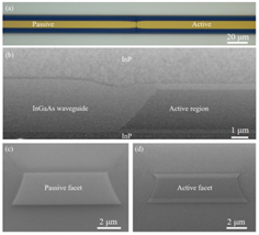
Some works have demonstrated the monolithic integration of QCLs with InGaAs passive waveguides on InP substrate, via an evanescent coupling and using QCLs with a 400-nm thick lateral SiN cladding [15]. However, to achieve high-performance and CW lasing operation, efficient optical coupling between active and passive waveguide sections, and semiconductor cladding to enhance the heat dissipation and low-loss passive waveguide is essential. In this regard, we have developed an integrated platform where light from an active QCL waveguide is coupled into a passive waveguide through a clean and smooth butt-joint, with negligible optical losses. The waveguide core material is undoped InGaAs, characterized by low free-carrier absorption, and experimentally showing losses of only 1.2 ± 0.3 dB/cm. To improve the heat extraction from the active section, both active and passive sections have InP semiconductor cladding.
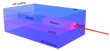
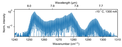
Thanks to this unique approach, we could demonstrate a QCLs lasing at room temperature and in CW operation around the 8 μm wavelength. This CW operation mode, together with a weak cavity dispersion, allowed the experimental observation of frequency comb formation over a broad optical spectrum of approximately 60 cm−1, which was verified by directly measuring the intermodal beatnote [16] and beatnote interferometry technique [17]. The cavity length of the device is directly related to the spectral spacing between comb lines. It means that, the longer the cavity is, the more dense comb formation is achieved. Interestingly, thanks to the smooth active-passive coupling with negligible losses, this work managed to extend a 3 mm active section with a passive waveguide of 2 mm. In this way, a denser comb was successfully achieved, with a similar current injection and heat dissipation requirements.
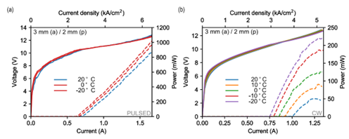
In conclusion, we have demonstrated the monolithic integration of mid-infrared QCLs with low-loss passive waveguides. The passive waveguide is fabricated by wet etching and selective area growth techniques. A clean and smooth butt joint between the active section and low-loss passive waveguides (1.2 ± 0.3 dB/cm). We report CW lasing of a 3 mm long active and 2 mm passive section device, showing a frequency comb operating near 8 µm wavelength. Moreover, our approach involves the growth of the active material and passive waveguide in separate steps, enabling a high flexibility in epitaxial layer and waveguide structure design. Also, the fabrication process that we have developed is highly tolerant to misalignment between different layer masks. Therefore, this work is a major advance toward mid-infrared PICs, as this platform enables fully integrated on-chip spectroscopic sensors.
Our research article about this RF-enhanced comb properties can be found external page here.
References:
(1) Smit, M.; Williams, K.; van der Tol, J. Past, present, and future of InP-based photonic integration. APL Photonics 2019, 4, No. 050901.
(2) Tombez, L.; Zhang, E. J.; Orcutt, J. S.; Kamlapurkar, S.; Green, W. M. J. Methane absorption spectroscopy on a silicon photonic chip. Optica 2017, 4, 1322−1325
(3) Coldren, L. Monolithic tunable diode lasers. IEEE J. Sel. Top. Quantum Electron. 2000, 6, 988−999.
(4) Wang, Z.; Van Gasse, K.; Moskalenko, V.; Latkowski, S.; Bente, E.; Kuyken, B.; Roelkens, G. A III-V-on-Si ultra-dense comb laser. Light: Sci. Appl. 2017, 6, e16260−e16260
(5) Gordon, I.; et al. The HITRAN2016 molecular spectroscopic database. J. Quant. Spectrosc. Radiat. Transfer 2017, 203, 3−69
(6) Faist, J.; Capasso, F.; Sivco, D. L.; Sirtori, C.; Hutchinson, A. L.; Cho, A. Y. Quantum Cascade Laser. Science 1994, 264, 553−556.
(7) Yao, Y.; Hoffman, A. J.; Gmachl, C. F. Mid-infrared quantum cascade lasers. Nat. Photonics 2012, 6, 432−439.
(8) Razeghi, M.; Lu, Q. Y.; Bandyopadhyay, N.; Zhou, W.; Heydari, D.; Bai, Y.; Slivken, S. Quantum cascade lasers: from tool to product. Opt. Express 2015, 23, 8462−8475.
(9) Villares, G.; Hugi, A.; Blaser, S.; Faist, J. Dual-comb spectroscopy based on quantum-cascade-laser frequency combs. Nat. Commun. 2014, 5, 5192.
(10) Spott, A.; Peters, J.; Davenport, M. L.; Stanton, E. J.; Merritt, C. D.; Bewley, W. W.; Vurgaftman, I.; Kim, C. S.; Meyer, J. R.; Kirch, J.; Mawst, L. J.; Botez, D.; Bowers, J. E. Quantum cascade laser on silicon. Optica 2016, 3, 545−551.
(11) Nguyen-Van, H.; Baranov, A. N.; Loghmari, Z.; Cerutti, L.; Rodriguez, J.-B.; Tournet, J.; Narcy, G.; Boissier, G.; Patriarche, G.; Bahriz, M.; Tournié, E.; Teissier, R. Quantum cascade lasers grown on silicon. Sci. Rep. 2018, 8, 7206.
(12) Go, R.; Krysiak, H.; Fetters, M.; Figueiredo, P.; Suttinger, M.; Fang, X. M.; Eisenbach, A.; Fastenau, J. M.; Lubyshev, D.; Liu, A. W. K.; Huy, N. G.; Morgan, A. O.; Edwards, S. A.; Furlong, M. J.; Lyakh, A. InP-based quantum cascade lasers monolithically integrated onto silicon. Opt. Express 2018, 26, 22389−22393.
(13) Radosavljevic, S.; Radosavljevic, A.; Schilling, C.; Hugger, S.; Ostendorf, R.; Kuyken, B.; Roelkens, G. Thermally Tunable Cascade Laser With an External Germanium-on-SOI Distributed Bragg Reflector. IEEE J. Sel. Top. Quantum Electron. 2019, 25, 1−7.
(14) Montoya, J.; Wang, C.; Goyal, A.; Creedon, K.; Connors, M.; Daulton, J.; Donnelly, J.; Missaggia, L.; Aleshire, C.; Sanchez-Rubio, A.; Herzog, W. Integration of quantum cascade lasers and passive waveguides. Appl. Phys. Lett. 2015, 107, No. 031110.
(15) Jung, S.; Palaferri, D.; Zhang, K.; Xie, F.; Okuno, Y.; Pinzone, C.; Lascola, K.; Belkin, M. A. Homogeneous photonic integration of mid-infrared quantum cascade lasers with low-loss passive waveguides on an InP platform. Optica 2019, 6, 1023−1030
(16) Soref, R. Mid-infrared photonics in silicon and germanium. Nat. Photonics 2010, 4(8), 495–497.
(17) Villares, G.; Riedi, S.; Wolf, J.; Kazakov, D.; Süess, M. J.; Jouy, P.; Beck, M.; Faist, J. Dispersion engineering of quantum cascade laser frequency combs. Optica 2016, 3, 252−258.
(16) Hugi, A.; Villares, G.; Blaser, S.; Liu, H. C.; Faist, J. Midinfrared frequency comb based on a quantum cascade laser. Nature 2012, 492, 229−233.
(17) Burghoff, D.; Yang, Y.; Hayton, D. J.; Gao, J.-R.; Reno, J. L.; Hu, Q. Evaluating the coherence and time-domain profile of quantum cascade laser frequency combs. Opt. Express 2015, 23, 1190−1202.